
When assembling equipment a tedious and time consuming task is creation of wiring looms and wiring front panel IO. Over the past two years the electronics section where I work has been trying to do away with it.
Our section has made the switch for 90% of the designs we do and it has massively reduced the time of the builds especially when the quantity is greater than one.
Its has however taken a while to get to the point where we’re efficient at using PCB mount IO for external and internal IO for multiple reasons. I’ll go through a few on them here to let you know what you’re in for.
Enclosure Selection
Selecting the correct enclosure is a time consuming task no matter how you assemble your equipment. I personal insist on aesthetics; the end user will and do rate the equipment on aesthetics and then functionality. If the enclosure is too large the equipment will look silly and too small you’re going to have serious issues.
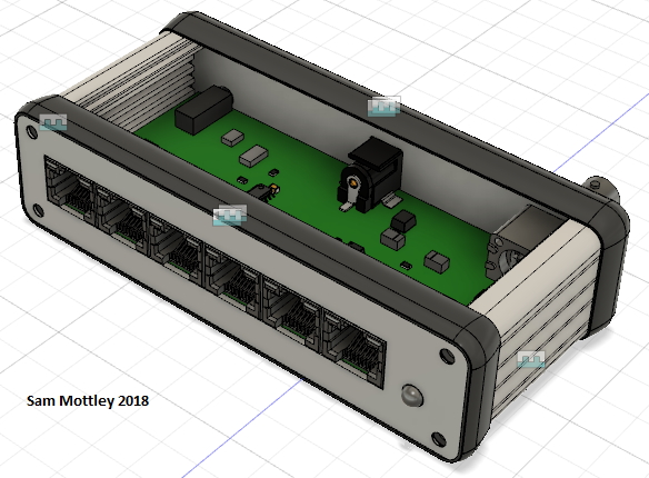
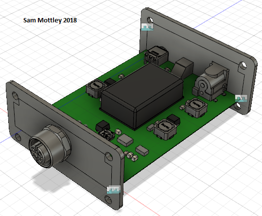
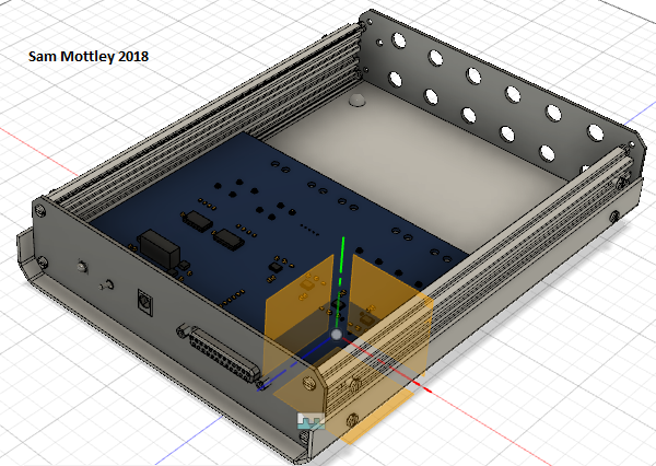
When selecting an enclosure for PCB mount components the list of enclosures gets even smaller. To save you time and hair loss I suggest you select one where the front and rear panels are completely removable and preferably if the lid can be removed as well even better. One example I’m missing but will work is where only the lid is removable and you only require one side to have IO (kind of like example 3). A common example of this type is a rack mount enclosure; it would be rare your PCB spans a full length of a 19″ rack mount enclosure.
To make it even more annoying when selecting an enclosure, try finding one where the manufacturer will provide STL (3D) models of the enclosure. Most enclosure companies are not providing these on their website, however i have found that emailing them can often help.
| 1. Front, rear and lid removable | 2. Front and rear panel removable. | 3. All panels removable |
 |
 |
 |
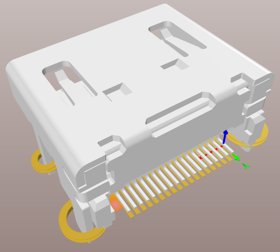
3D Component Footprints
3D design is ultra critical when designing for front panel IO. That goes for your PCB design using accurate 3D models for components to the manufacture of your enclosure providing 3D models.
This meant that as a Section we had to ensure all components made and used from that moment onward had a 3D model. This is not hard to do and actually helps. Pretty much all manufacturers of components provide a 2D drawing of the component for the footprint and now a 3D model in STL format. When designing the footprint you use the 2D drawing and then you insert the 3D model. A bonus to this is once the 3D model is loaded you can then use it to check your footprint see below ;).
Suggestion: Purchase a Nerf and pop anyone who does not use a 3D model in your shared library. Its that important! Life and dead people. #Joke but serious it’s important.
| HDMI Connector 2D | HDMI Connector 3D |
 |
 |
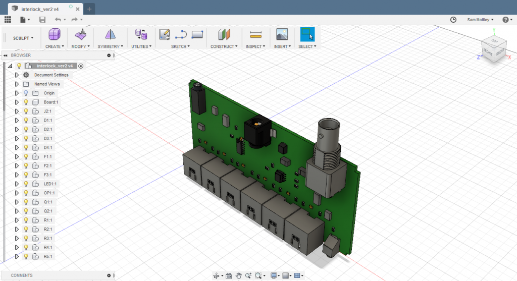
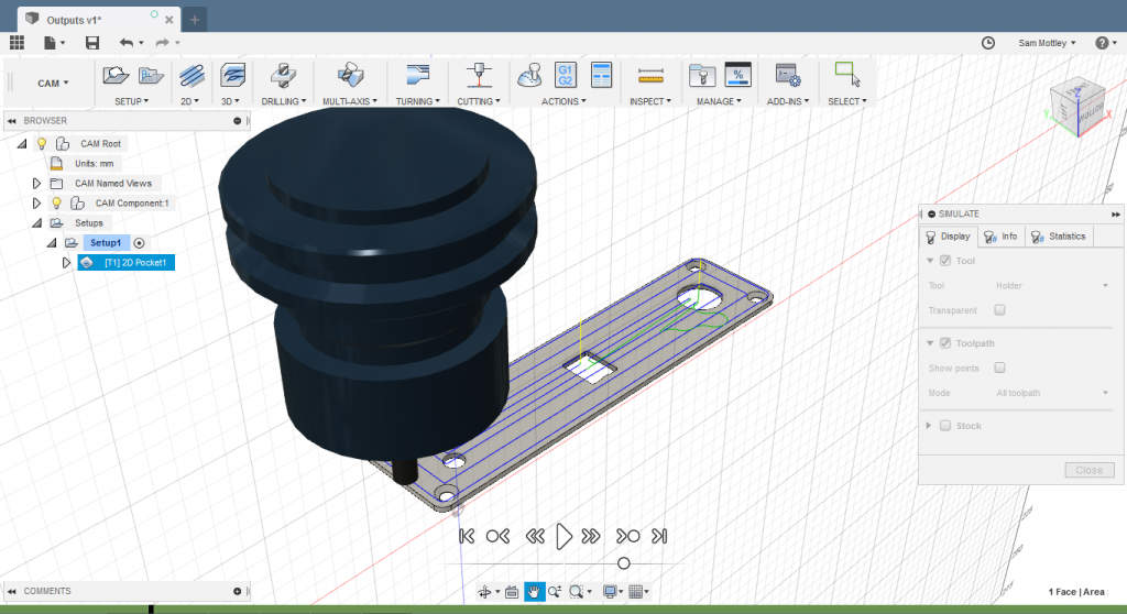
Any way, once all your components have 3D model’s, and you have completed you PCB design, then you can export an STL of your PCB. This file is a 3D model of your PCB which can be loaded into a 3D design package like so:
CAD
With the above two steps you now have your PCB and enclosure imported into your selected 3D design software. It is then a simple process to edit the required panels to have the desired cut outs for your PCB as you can visually check your modifications, for example:
However, when I joined the Electronics Section I was already quite fluent in CAD using Solidworks. So the above was an easy and quick task for myself. Ultimately everyone had to learn the process and not just me, which took a awhile, but now 2 years on is an doable task for everyone.
I highly suggest using Fusion 360 for your 3D design package due to its easy to use interface and community. I’ll make a short post on the quickest method of doing front panels soon.
CAM
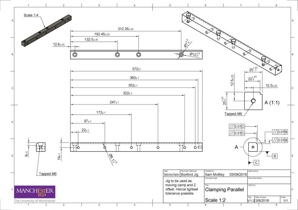
Once you have your 3D design using CAD there are two methods you can go down. The first method is making a 2D drawing of your front panel and send it to a mechanical workshop or build it yourself, below is an example 2D drawing I had on hand:
The second method is to use CAM or “Computer Aided Manufacture”. This is where you take your 3D drawing and create tool-paths for a CNC machine to manufacture your panels. This type of work can be done from within good CAD packages such as fusion 360.
Recently as a couple of months, our section has bought a Boxford CNC Router. This will route everything up to non-ferrous metals, such as Aluminium, Copper, Brass. Which happens to be the most common metals we in the Electronics Section work with. You can build a really good cnc router capable of cutting metal for around £2000 or purchase a cheap one for around the same price. I suggest buying one with linear ground rails and ball screw drives.
Design Methodology
The last point I’ll touch up on is you really have to change the way you think about designing your equipment. You have to think hard about your end enclosure design as much as you do the PCB design.
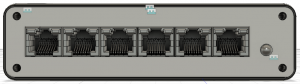
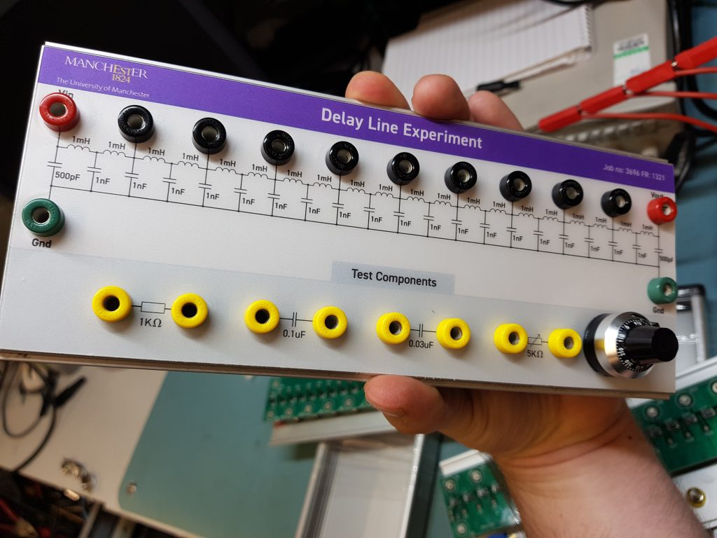
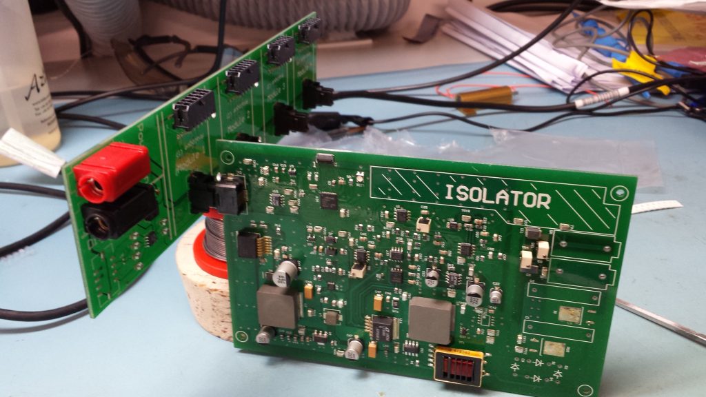
Example 1: When selecting a connector you not only need to spec the electrical side but also how rugged the mounting is to the PCB. As this connector is not going to experience the real world of end users, arhh. Below is a quirky example of how to use banana sockets.
| Top | Bottom |
 |
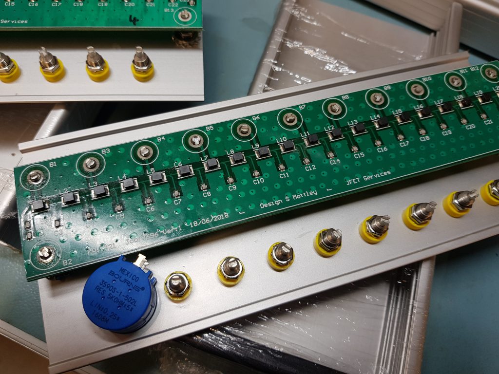 |
Example 2: Your PCB shape will play a critical role. You can’t just plonk your PCBs into a large enclosures and sling some wires around. Your PCB shape now needs to fit into the enclosure and panels like a hand into a slim glove.
Example 3: More a tip than an example but try designing your PCB shape and positions of IO in your CAD package and then create a dxf to import into your PCB design software. This will help fix your IO in their required position and stop temptation to move things out of alignment for easy routing we’re watching you.
Example 4: Try and use digital buses instead of analogue signals as this gives you the ability to run back planes
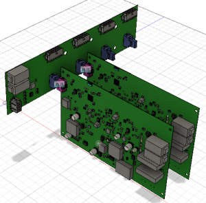
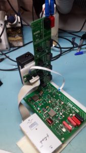
| 3D Assembly | Desk Assembly | Test Rig Assembly |
 |
 |
 |


