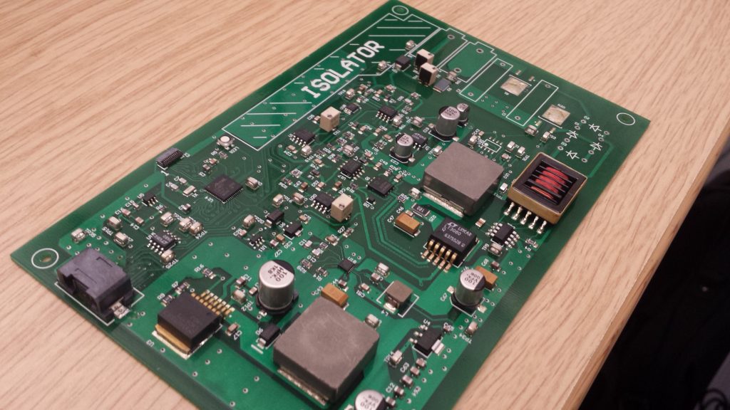
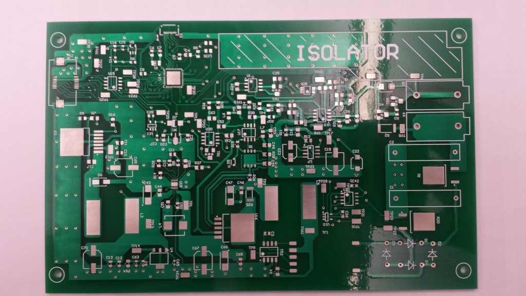
I joined The University of Manchester’s Electronics Section around 5 years ago now. When I arrived the Section was still using through hole components. After a lot a pushing the section slowly made the transition to SMD components, and have never looked back since. Don’t get me wrong there are situations where through hole components are required.
Putting aside the electrical advances of SMD components, one of the biggest advances is how you assemble your PCBs. When assembling boards I really dislike through hole components, and so will you when you make the switch. It simply takes twice as long to assemble and create an array of metal legs all over your desk. There are two methods of assembling SMD PCBs which I’ll explain in detail below.
Method 1: Hand soldering
This is the obvious one! There is a myth that SMD components are just too hard to hand solder and you need a machine. I can confirm this is complete rubbish. Don’t let poor eye sight put you off either, the average age in our section is around 55 and no one has issue with hand SMD soldering.
The process of hand soldering board:
- Tin one pad on the component footprint
- Apply flux (not necessary)
- Using SMD tweezers move the component on top of the footprint
- Continue holding the component while touching the tinned pad + smd leg/pad with your soldering iron
- Continue holding the component until solder sets.
- NOTE: Do not blow on solder to cool it faster. This can cause dry joints.
- Wise off the fluke and apply new flux (not necessary)
- Solder each leg/pad as now the component will be rigid to the PCB
- Re-solder the first pad as often its not a very good joint.
A piece of advice buy some quality SMD tweezers; for a set they’ll often cost £60.
Once you’ve got the hang of this method I can guarantee it will be quicker than through hole assembly. However it’s scary how many people and small companies stick to this method. Yes it’s quick but its not as quick as it can be!
Method 2: Re-flowing
Are re-flowing boards, like the transition from hell to purgatory to heaven. The re-flow process will speed up your assemble time hugely however there is a major down side. Unlike hand assembly you can’t test your board or your assemble section by section. You end up with a fully assembled board.
First though check for bug problems as most of the work I do is prototype. However its easily fixable by following the below two tips.
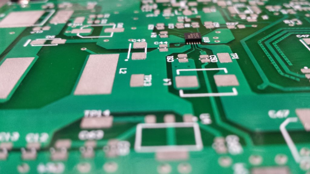
- Test points I do lots of them. SMD is so small we using Harwin test points. They are SMD and have three sizes, the smallest being almost the same size as your PCB traces. Hence they really don’t get in the way of routing, use them!
- Links, these are a simply two pads very close together. Which you can short with a blob of solder and separate with some wick. Using these inline with traces and to power pins allow you to separate parts of your circuit after assembly.
Below goes through the re-flow processes:
Clean you PCB using IPA
Aligning a stencil over your PCB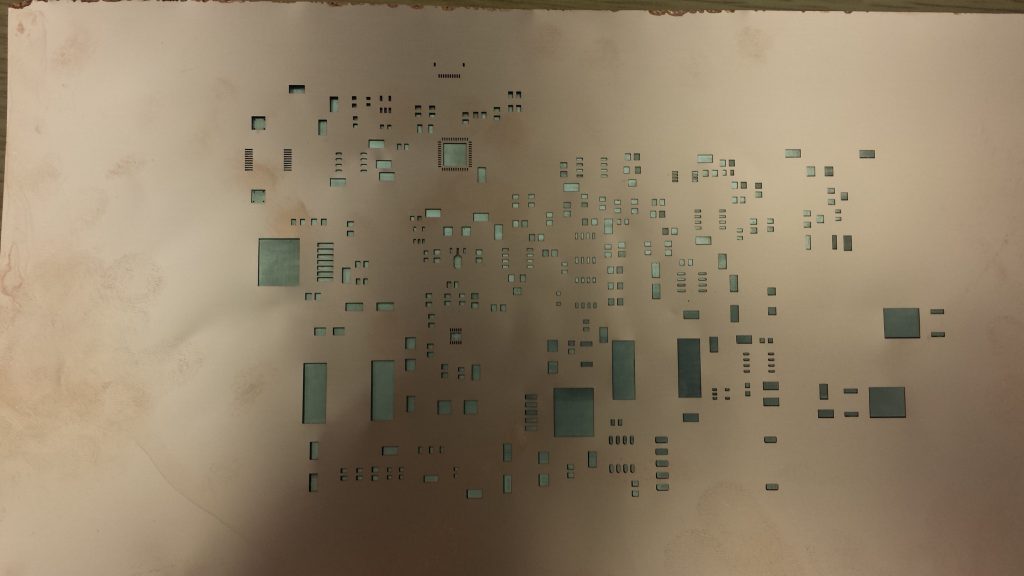
Next tape the mask down and using a squeeze or credit card etc spread solder paste over the stencil. Once you have a even coat remove the stencil and you’ll have a PCB with solder paste on the pads.
You then place all your SMD components on to the PCB using tweezers
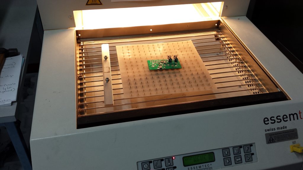
Finally you put your board into a re-flow oven.
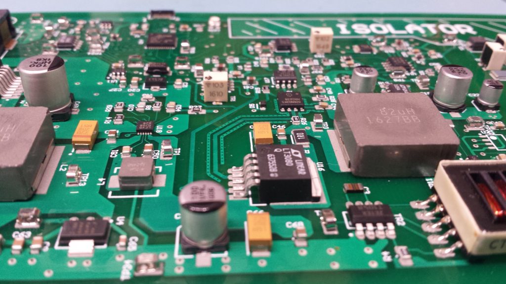
Below shows a professional oven (different board I built), however in our workshop we built our own oven which I’ll post up soon. Budget around £100-£200 to build your own oven on the cheap.
And you’re done!
If your ever going to listen to a stranger on the internet, then this is the post you should listen to. Invest the time and make the transition to re-flowing.