
Currently I’m designing a power supply board for a vacuum reservoir system. I have a 24V power supply and need to generate plus and minus 5V for some analogue + digital circuitry.
Normally I would use off the shelf DC-DC that can provide a couple of mA; however this time i want to my +-5V supplies to have some reasonable drive capacity for future expansion.
There is the obvious method of using a transformer based solution but I didn’t want to do this, mainly due to cost and size footprint. In the past I’ve used switched capacitor voltage inverters. However generally speaking they are not capable of over 250mA.
Solution: Buck Regulator
Inverting a positive voltage to a negative one can be performed by most buck regulators. However be careful as some may not work due to internal protection / compensation inside the IC.
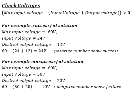
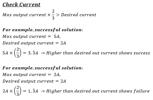
I decided to use a Texas buck regulator TPS54560B which can take between 4.5-60V input and is capable of 5A continuous output current. However, when configured into a negative output voltage these limits are slightly reduced as a rule of thumb I use the following:
Selecting component values
After you have made sure that the IC will cope with your conditions under a negative configuration, you can design your circuit. The design process for selecting component values are identical in both configurations. Just follow along with the datasheet.
Schematic
Both configurations are wired up in an almost identical format. However there are a few slight differences for the negative supply that you have to take into account.
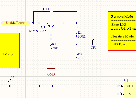
| Enable pin has be to lifted using a level shift as it will be reference to a negative voltage.
The circuit to the right allows a positive voltage to enable the IC when in a negative configuration. Negative Configurations Positive Configurations |
 |
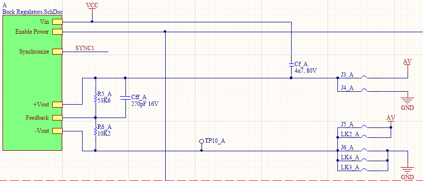
| The outputs have to be referenced differently.
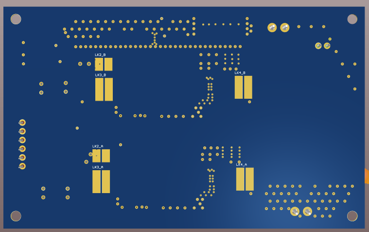
For negative configurations the output of the inductor is tied the common/ground and gnd on the IC now becomes a negative voltage. As you can see to the right I want to be able to switch configurations between positive and negative. Hence I use jumpers to tie each point to the correct location. |
 |
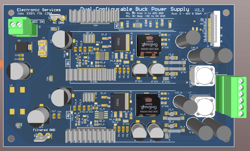
PCB layout
The layout of the PCB is important in order for the buck regulations to work efficiently. However to spice life up slightly, the aim to make each buck configurable into positive / negative mode makes the layout even more critical. Additional links were added to the schematics in order to match the polygon pours correctly.
| 2D | 3D | |
| Top | 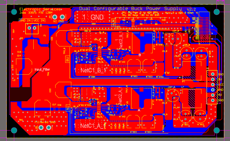 |
 |
| Bottom | 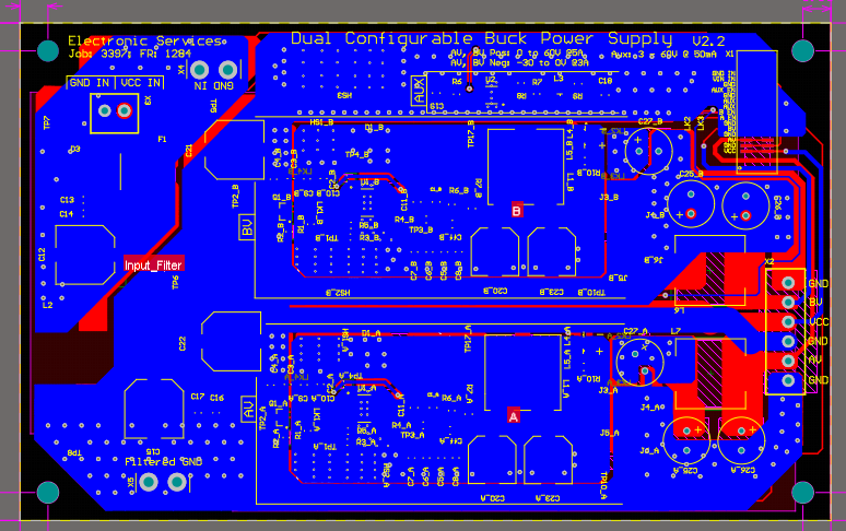 |
 |


